

If you build debug tools for a living, you have a recurring problem: you need hardware that does not exist yet. The RISC-V Vector Extension (RVV) is a good example. RVV is the part of the RISC-V instruction set architecture (ISA) that adds data-parallel computation, ratified as version 1.0 in late 2021. It is how RISC-V does the heavy lifting for signal processing, machine-learning inference at the edge, and any workload where one instruction should operate on a whole vector of values at once. Toolchains support it. Simulators support it. Our debug tools support it. But physical RVV 1.0 hardware that you can put on a desk, wire a probe to, and drive register-access tests against? That is still thin on the ground, and where it does exist, it tends to be a customer’s carefully guarded pre-production board.
So, when we wanted to exercise the vector register support in Ashling’s GDB server, part of our RiscFree SDK, against something real for a long-term customer, we took a different route: build the hardware ourselves, from open-source parts, on an FPGA board that costs a few hundred dollars.
This is the story of how that went. It went well, it went quickly, and it proved to be well within reach of engineers who would describe themselves as software people. That last point is the one we want to convince you of. Most of this work was done by an engineer with a software background, an AI assistant, and a Digilent board that had been sitting on a desk. No FPGA apprenticeship required.
Five characters carry this story: four of them open-source (or at least openly documented) hardware and tools, and one that is not hardware at all.
Vicuna (github.com/vproc/vicuna) is an open-source vector coprocessor written in SystemVerilog, originally developed at TU Wien. It implements the RVV 1.0 specification, specifically the Zve32x embedded profile, which supports integer vector operations on 8-, 16- and 32-bit elements and omits floating point. Crucially for us, Vicuna is not a whole CPU. It is a coprocessor that attaches to a host core through the CORE-V eXtension Interface (CV-X-IF), a standard socket by which a RISC-V core can delegate instructions it does not understand to something that does. Vector instructions flow across that interface to Vicuna; everything else runs on the host core as normal. Figure 1, taken from the project’s own documentation, shows the overall shape: instructions arrive over CV-X-IF, are decoded and dispatched to a configurable number of vector pipelines, and results flow back to the register files.
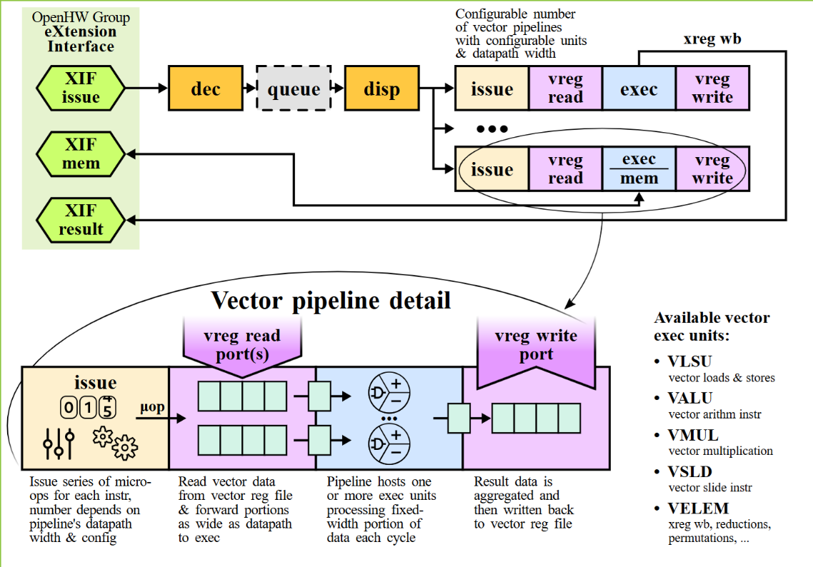
Figure 1: High-level overview of the Vicuna vector coprocessor (source: github.com/vproc/vicuna).
Ibex (github.com/lowRISC/ibex) is that host core: a small, production-proven, 32-bit RISC-V CPU (RV32IMC, the base integer set plus multiply/divide and compressed instructions) maintained by lowRISC, with a two-stage pipeline and a footprint small enough for almost any FPGA. Vicuna’s repository pins a lightly modified Ibex fork with the CV-X-IF socket wired in.
riscv-dbg (github.com/pulp-platform/riscv-dbg) is the PULP Platform’s implementation of the RISC-V Debug Specification (version 0.13), the piece that lets an external debugger halt the core, read and write its registers, and access its memory. More on this later, because the Vicuna demo design does not include it, and that absence is half the plot.
The Arty A7-100T (digilent.com) is Digilent’s popular development board built around a Xilinx (now AMD) Artix-7 XC7A100T FPGA in a CSG324 package: 101,440 logic cells, 240 DSP slices, 4,860 Kb of block RAM (BRAM), a 100 MHz reference clock, 256 MB of DDR3L, and USB connections both for configuring the FPGA and for UART communication with whatever you build inside it. A field-programmable gate array (FPGA), for the software readers, is a chip full of configurable logic: you describe a circuit in a hardware description language, tools compile that description into a bitstream, and the FPGA becomes that circuit. It is how you get to hold someone else’s CPU design from GitHub in your hand.
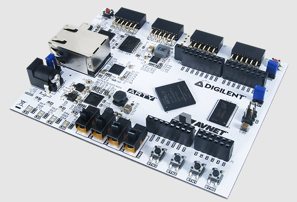
Figure 2: The $300 Digilent Arty A7-100T FPGA Board.
The design flow ran in Xilinx Vivado (amd.com/vivado), the standard toolchain for Artix-7 parts, which takes the SystemVerilog register-transfer level (RTL) sources through synthesis, placement, routing and bitstream generation.
And finally, Claude, Anthropic‘s AI assistant, played the role of the FPGA veteran we did not have in the room: the colleague who has read every datasheet and does not mind being asked, for the tenth time in a day, what a Vivado error message actually means. Claude helped us navigate the unfamiliar codebase, modify and build the design for our board, and integrate the debug hardware. Editor’s note: this story was drafted with Claude’s assistance. We are told the glowing character reference is a complete coincidence. Ok Claude, we get it. Enough already!
Vicuna ships with a small FPGA demo: a top-level module (demo_top.sv), a block-RAM main memory initialised from a .vmem file, and a UART. The whole design needs five pins (clock, reset, UART receive and transmit) and the Makefile generates a complete Vivado project. It is as gentle an introduction as FPGA projects offer. The catch: the demo’s .xdc constraint files, which tell Vivado which physical package pins the design’s ports connect to and what the board’s clock looks like, cover Digilent’s Nexys Video and Genesys 2 boards. Not the Arty A7.
This is the first place a software engineer might stall, and it turns out to be a bookkeeping problem rather than hardware wizardry. An .xdc constraint file is a few dozen lines and the Arty A7-100T’s reference documentation lists every pin, and the project’s existing constraint files provide the template. Adapting one for the Arty (its 100 MHz single-ended clock, its reset button, its USB-UART pins etc ), plus pointing the Makefile at the correct part number (xc7a100tcsg324-1), is an hour of careful cross-referencing, not months of Verilog.
It helped that we did not do the cross-referencing alone. This is where Claude earned its place in the cast: navigating the unfamiliar parts of the codebase, drafting the board constraints, and adjusting the build configuration, with every change checked against the board documentation. The AI designed no hardware. What it did was remove the “unfamiliar ecosystem” tax: the hours normally spent working out which of five similar files matters, and what a cryptic Vivado message is actually complaining about. For software engineers considering a project like this, that tax is most of the barrier, and it is now largely optional.
With constraints in place, Vivado completed synthesis and implementation, produced a bitstream, and the Arty came up running code from its block RAM: an Ibex core with a vector coprocessor alongside, talking to the world over UART. Figure 3 shows the finished Vivado project after the debug hardware (next section) had also gone in: synthesis and implementation both complete with no errors or warnings, in around five and a half minutes each, targeting part xc7a100tcsg324-1. Note the design hierarchy on the left, where the transplanted debug modules (u_dmi_jtag, u_dm_top) sit alongside Vicuna (vproc_top), the RAM and the UART interface, as if they had always been there.
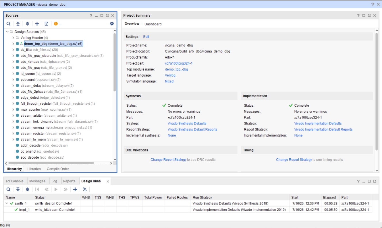
Figure 3: The ported project building cleanly in Xilinx Vivado for the Arty A7-100T.
A soft core running inside an FPGA is a black box within a black box. The Arty’s USB-JTAG connection configures the FPGA by loading the bitstream, but it offers no visibility into the processor built inside it. If your program misbehaves, a UART printf is the only window you have. Vicuna’s demo design, deliberately minimal, contains no debug hardware at all.
What a debugger needs on the far side of the cable is defined by the RISC-V Debug Specification, and it comes in two parts. The Debug Module (DM) sits inside the system next to the core: it can halt and resume the hart (RISC-V’s term for a hardware thread), feed it instructions, and reach into memory. The Debug Transport Module (DTM) is the DM’s connection to the outside world, in our case over JTAG (the venerable IEEE 1149.1 serial test interface), carrying a small register protocol called the Debug Module Interface (DMI) between the probe and the DM.
We wrote none of this; we transplanted it. The PULP Platform’s riscv-dbg repository provides exactly these two modules, already proven in cores such as Ibex and CVA6, which meant the integration points were well documented. In went dmi_jtag.sv (the DTM, with its JTAG test access port) and dm_top.sv (the DM), wired into the demo system’s bus alongside the RAM and UART, with the DM’s debug request line connected to Ibex.
One architectural point is worth noting: riscv-dbg uses an execution-based debug scheme. When you halt the core, it does not freeze in place. It is redirected into a “park loop” inside a small debug ROM, where it sits awaiting instructions. When the debugger wants to read a register, the DM places the corresponding instruction into a program buffer and has the core execute it on its own behalf. It is a clever inversion (the core debugs itself, under supervision) and it keeps the intrusion into the core’s own RTL small, which is exactly what you want when grafting debug logic onto someone else’s design.
The last piece was physical. riscv-dbg offers two flavours of JTAG tap: one that piggybacks on the FPGA’s own configuration JTAG (using Xilinx BSCANE2 primitives), and a full pin-level test access port. We chose the pins: the soft core’s JTAG signals (TCK, TMS, TDI, TDO) were routed out through one of the Arty’s PMOD expansion headers, giving a real debug connector for a real external probe. That choice matters: it means the target presents to a debug probe exactly as production silicon would. Same wires, same protocol, no FPGA-specific tricks in the path.
We promised to be clear about where the effort went, so here is the one place the bring-up pushed back. It was not a bug, strictly. It was more useful than a bug: a lesson about the seams between IP blocks, of the kind only real hardware teaches. First contact between debugger and target was not clean. Debug operations were returning a status of “busy” when the debugger expected them to be complete, along with occasional error responses. To see why, you need one more piece of JTAG anatomy. When a debugger issues a Debug Module Interface operation, it shifts the request in through the JTAG state machine and then parks in a state called Run-Test/Idle (RTI) for a few clock cycles while the chip performs the operation. How many cycles should it wait? The DTM itself advertises the answer, in a small field called idle in its dtmcs (DTM Control and Status) register. The upstream dmi_jtag.sv ties that field to 1, promising that a single idle cycle suffices.
For this integration, it did not. The debug request must cross from the JTAG clock domain (a modest 1 MHz) into the core’s clock domain, and it makes that crossing through a genuine two-phase asynchronous handshake in dmi_cdc.sv, a clock-domain crossing (CDC) that needs more than one round trip to settle. The probe, taking the DTM at its word, returned after one idle cycle and found the operation still in flight: “busy”, or worse, the specification’s error code for “too fast”. The fix was one line: advertise idle as 7, so that any conforming debugger waits long enough. The symptom disappeared, confirmed by live testing on the board in both directions: busy and error responses with the old value, none with the new.
Two things about this episode are worth recording. First, it is not really a defect in riscv-dbg: an integration with a tighter clock-domain relationship may be perfectly content with 1. It is an integration parameter disguised as a constant, and it only reveals itself when a real probe drives real JTAG against a particular arrangement of clocks. That is precisely the class of issue this project exists to surface. Second, the tooling caught its own case: the debugger’s complaints were the diagnostic, and the fix now sits in the RTL beneath a thorough explanatory comment drafted by Claude (Figure 4), so the next engineer to open the file gets the whole story.
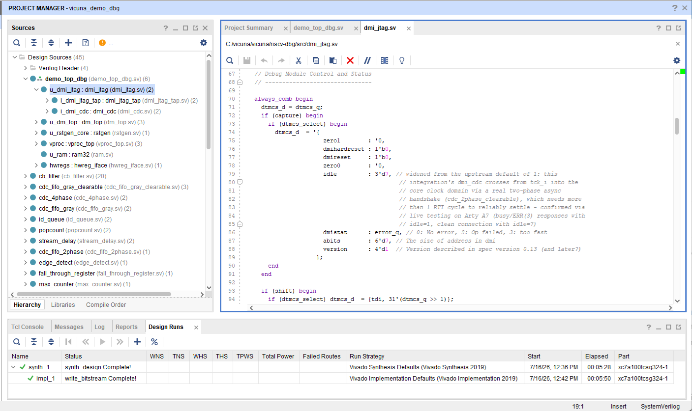
Figure 4: The one-line idle bitfield change in dmi_jtag.sv, with its Claude-drafted comment explaining why (shown in the Vivado editor).
With the augmented bitstream loaded, we connected an Ashling Vitra-XS debug probe to the PMOD JTAG header and pointed the RiscFree GDB server at it.
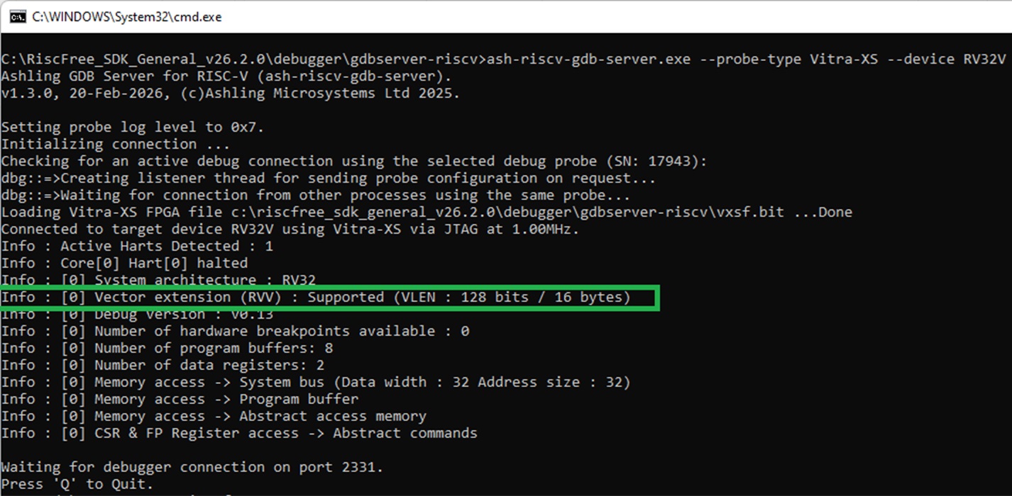
Figure 5: Ashling GDB Server console output on first clean connection to the Arty A7 target.
The console output (Figure 5) is worth reading line by line, because each line can be checked against the design. The server connects over JTAG at 1 MHz (deliberately modest; the debug logic requires the JTAG clock to run slower than the system clock, and bring-up is no time for ambitious clock rates). It detects one hart, halts it, and identifies an RV32 architecture. Then the line we built all of this for: Vector extension (RVV) : Supported (VLEN : 128 bits / 16 bytes). That is the GDB server discovering, by probing live hardware, that this target has vector registers 128 bits wide.
The rest of the readout matches the transplanted debug IP to the digit, and this is the kind of cross-checking that builds trust in a bring-up. Debug specification version 0.13: precisely what riscv-dbg implements. Eight program buffers, two data registers: hard-coded constants in the repository’s dm_pkg.sv. Memory access available via system bus, program buffer and abstract commands; register access via abstract commands. And one honest zero, “Number of hardware breakpoints available: 0”, because riscv-dbg does not include the optional trigger module, so breakpoints on this target are the software kind. The log and the source agree completely, which is exactly what you want to see before trusting a target with real test workloads.
From there, GDB connected to the server’s port and we ran what we came for: vector register access tests, writing patterns into the vector register file, reading them back and comparing. Initial results: clean. A debugger, a probe and an open-source vector core from GitHub, all in agreement about the contents of 128-bit registers, on a board that costs less than the shipping on some silicon evaluation platforms.
The immediate win is obvious: our GDB server’s RVV support was exercised against real hardware, with real JTAG timings, real DMI transactions and real vector state, rather than a simulator’s polite approximation.
But the pattern generalises, and this is the thought we want to leave you with. An FPGA board plus open-source cores is a configurable test-target factory. Need a different vector length? Vicuna’s VLEN is a build parameter; regenerate the bitstream. Want to test against a different host core? The demo supports swapping Ibex for CV32E40X with a Makefile variable. Different memory widths, different pipeline options: parameters. For anyone building or validating debug and development tools, this inverts a long-standing constraint. Instead of test coverage being limited by whatever silicon you happen to possess, you synthesise the target you need. Features can be tested before matching production silicon exists at all, which, in the debug-tools business, is remarkably often the position you are in.
And the barrier really has dropped. Every hardware ingredient in this story is open source and permissively licensed. The board is a stock item. The FPGA tools are a free download at this device size. The genuinely arcane knowledge (which file, which pin, which constraint) has become far more navigable with an AI assistant to hand. The result was achieved by software-first engineers in days rather than months.
There has never been a cheaper time to hold someone else’s processor in your hand, and to be able to look inside it while it runs.
Questions? We’d love to hear from you and please send your questions or comments to: engineer@ashling.com